
TL;DR
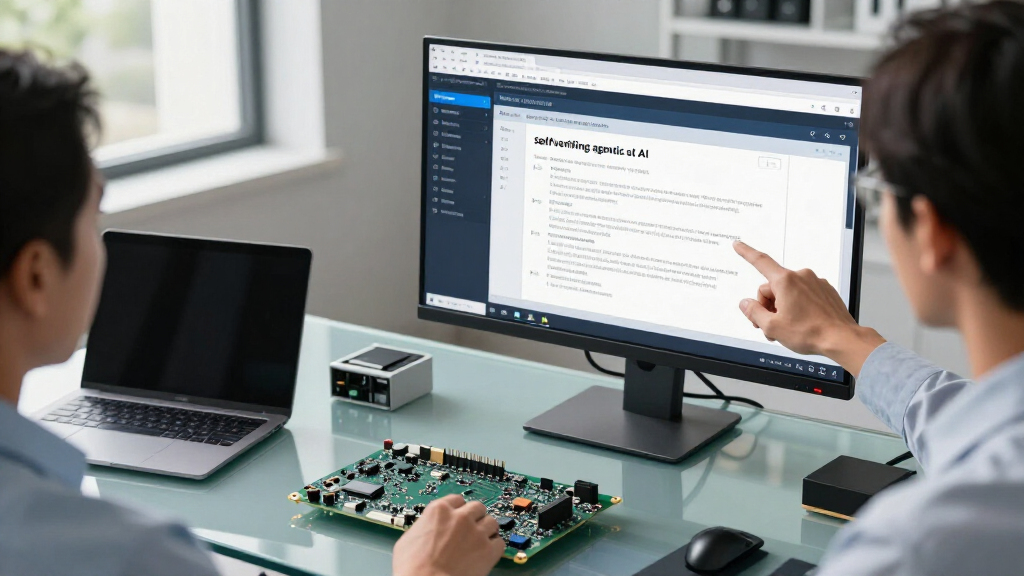
Siemens has announced the development of self-verifying, agentic AI workflows aimed at automating and streamlining semiconductor and PCB design. This innovation seeks to improve accuracy and efficiency in electronics manufacturing. The technology is in the early stages of deployment, with broader adoption expected in the coming months.
Siemens has introduced a new self-verifying, agentic AI workflow platform designed for semiconductor and printed circuit board (PCB) design. This development aims to automate complex design verification processes, potentially reducing errors and increasing productivity in electronics manufacturing. The announcement highlights Siemens’ push toward more autonomous, reliable AI-driven design tools, with initial deployment phases beginning in early 2024.
The new AI workflows from Siemens incorporate self-verification capabilities that allow the system to independently check and validate design outputs during the creation process. According to Siemens, these workflows are built to adapt and improve over time, leveraging agentic AI features that enable the system to make autonomous decisions within predefined parameters. The platform is targeted at semiconductor manufacturers and PCB designers seeking to streamline production and reduce costly errors. Siemens states that early testing has demonstrated promising results in reducing manual verification efforts and accelerating development cycles, though full-scale deployment is still in progress.Industry experts note that this technology aligns with broader trends toward automation in electronics manufacturing, where AI is increasingly used to handle complex design tasks. Siemens’ approach emphasizes self-verification as a key differentiator, aiming to minimize human oversight and enhance reliability. The company has not yet disclosed specific technical details or timelines for widespread adoption but indicated that the platform will undergo further testing before commercial release.
Potential Impact of Self-Verifying AI on Electronics Manufacturing
This innovation could significantly influence the electronics industry by reducing design errors and speeding up production cycles. Automated, self-verifying AI workflows may decrease reliance on manual checks, lowering costs and improving product quality. If successfully scaled, Siemens’ technology could set new standards for autonomous design verification and inspire similar developments across the sector, ultimately impacting supply chains and product timelines.

Static Timing Analysis for Nanometer Designs: A Practical Approach
As an affiliate, we earn on qualifying purchases.
As an affiliate, we earn on qualifying purchases.
Growing Adoption of AI in Semiconductor and PCB Design
Over recent years, the electronics manufacturing industry has increasingly integrated AI tools to enhance design accuracy and efficiency. Major companies have invested in machine learning models to automate routine tasks and improve defect detection. Siemens’ latest development builds on this trend, emphasizing self-verification as a means to further reduce human intervention and error. Prior to this, Siemens has been active in developing AI-driven automation solutions, but the focus on agentic, self-verifying workflows marks a notable advancement in their offerings.
The move aligns with industry-wide efforts to achieve higher levels of automation amid growing complexity in semiconductor and PCB designs, where traditional manual checks are time-consuming and prone to mistakes.
“Our new AI workflows are designed to enable autonomous verification, reducing manual effort and increasing reliability in semiconductor and PCB design.”
— Siemens spokesperson

The Complete KiCad 10 Handbook: Master PCB Design, Printed Circuit Board Development, Schematic Design, Electronic Circuits, and Hardware Prototyping from Scratch
As an affiliate, we earn on qualifying purchases.
As an affiliate, we earn on qualifying purchases.
Technical Details and Deployment Timeline Still Unclear
Siemens has not disclosed specific technical specifications or detailed timelines for when the self-verifying AI workflows will be commercially available. It remains unclear how the platform will integrate with existing design tools or the extent of its autonomous capabilities. Additionally, the readiness of the technology for large-scale industrial deployment is still under evaluation, and further testing phases are anticipated.

Analytical Skills for AI and Data Science: Building Skills for an AI-Driven Enterprise
As an affiliate, we earn on qualifying purchases.
As an affiliate, we earn on qualifying purchases.
Next Steps Include Broader Testing and Industry Adoption
Siemens plans to continue testing the AI workflows with select partners, aiming for broader industry trials in the coming months. The company has indicated that a commercial release could occur within the next year, contingent on successful validation and integration. Industry observers will be watching for updates on technical performance, user feedback, and the platform’s impact on design workflows.
As an affiliate, we earn on qualifying purchases.
Key Questions
What are self-verifying AI workflows?
Self-verifying AI workflows are systems that can independently check and validate their own outputs during the design process, reducing the need for manual oversight.
How will this impact semiconductor and PCB design?
It could increase automation, reduce errors, and speed up development cycles, leading to cost savings and higher quality in electronics manufacturing.
When will this technology be widely available?
Siemens has not provided a specific release date, but industry trials are expected to expand over the next few months, with a potential commercial launch within a year.
What are the potential challenges of implementing this AI technology?
Technical integration with existing tools, ensuring reliability at scale, and gaining industry trust are key hurdles that Siemens and others will need to address.
Source: primary